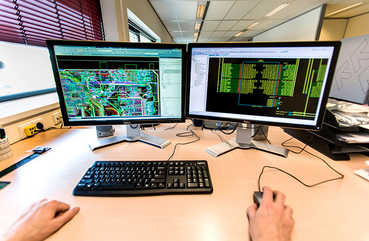
FPGA/SoC design
Adeas the specialists
Contact us for e.g.:
More and more functionality in a single device
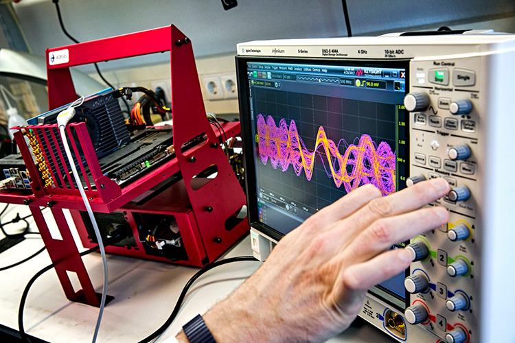
FPGA & SoC’s keep increasing in available resources, speed, and onboard hardcoded functionality. The sheer number of logic cells, transceivers, DSP cores, processors and IP available in today’s powerful devices, make it possible to implement more and more functionality in a single device. Users can integrate IP cores available through the component vendors and third parties with their own designs like never before. The drawback is the ever-increasing amount of human resources to complete such large and complex designs. Advanced tools allowing a higher level of programming helps counter this development, but it’s the thorough understanding of system requirements, tools and low-level device characteristics that Adeas offers that ensures a successful design.
Our knowledge and experience with the ins and outs of the latest components, tools, and possibilities enable us to implement even the most complex algorithms, control and high-speed interface.
Longstanding partnerships
Adeas has longstanding design partnerships with AMD Adaptive and Embedded Computing (formerly Xilinx) and Intel Programmable Solutions (formerly Altera) which enables us to access the latest roadmap information, IP cores, component samples and high priority support. It also ensures continuous education and training of our engineering staff on design tools and component capabilities and architecture.
Through the extensive experience of our specialists with the component families of the market leaders and the (im-) possibilities of the design tooling, we are able to choose the direction toward an optimal solution in an early stage. This is especially important when meeting challenges with clock domain issues, signal filtering, resource reduction and timing requirements. We are also familiar with the pitfalls and are able to avoid these to our and our clients’ advantage.
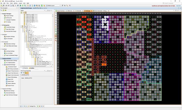
RTL or high-level language
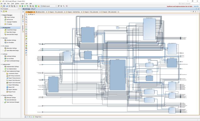
To get the most out of a device in terms of efficiency, resource usage and speed it is often necessary to code the FPGA fabric at register-transfer level (RTL). To do this we are proficient in VHDL and (System) Verilog. Though often the top level of a design is made with a graphical entry tool to be able to quickly oversee a system and its interfaces and discuss this with system
level designers and architects of our clients. Depending on the requirements of a project and the targeted FPGA it can be a good idea to use a high-level language like C in combination with a tool to automatically generate RTL to program an FPGA. This can, for instance, be very helpful and drastically shorten the lead time when optimising algorithms that are subject to change while evaluating. In its projects, Adeas carefully considers which way to go to ensure our customer gets maximum value.
SoC
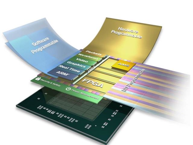
Increasingly FPGA fabric is combined with advanced hardcore processors to form a System on Chip (SoC) This enables the real-time FPGA logic to be combined with the versatility of powerful ARM and Intel processors. With optimal interconnect between FPGA fabric and processor(-s) this combination is especially suitable for applications where hardware acceleration is required for processing tasks that would need too much processing power of the processor, or for functions that cannot be handled by a processor, e.g. due to critical timing behaviour or high bandwidths.
Typically in SoC programming, we form an engineering team comprising of lead designer or architect to oversee the system with software and FPGA firmware professionals that work closely together. This is necessary to achieve an optimal result in even the most challenging designs.
IP development and Integration
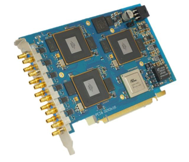
The term IP (Intellectual Property) core is used for a commercially available block of code especially designed for use in an FPGA, SoC or ASIC. An IP core performs a certain function when fitted in such a device and can accelerate the development lead time of a customers project by saving engineering time and -resources. The FPGA companies (Xilinx, Intel, Lattice, Microsemi etc.) provide IP suitable for use in their devices but there are also third parties selling IP cores. Adeas has extensive experience with the selection, use and integration of many IP cores available today.
We use them with the complicity and to the advantage of our customers. Adeas also has a modest IP core portfolio for which licenses can be bought.
Tooling
At Adeas we use a whole range of tools that enable us to design, simulate and integrate better, faster and with high quality. However, our experts know what the tooling is capable of and what to choose for the specific requirements of a project.
| Xilinx Vivado ™ |
| Vivado ™ HLS |
| PlanAhead ™ |
| ISE ® |
| SDAccel |
| MicroBlaze ™ |
| PicoBlaze ™ |
| EDK/SDK |
| Quartus ® II |
| Modelsim ® |
| Questasim ® |
| NC-Sim ® |
| Verilog-XL |
| Synplify Pro ® |
| Synopsys Design Compiler ® |
| Matlab ® |
| Simulink ® |
| HDLdesigner ® |
Embedded System Design
At the start of an embedded system project, we form a team consisting of hardware, software and firmware specialists guided by a lead designer or system architect. The system architect is responsible for the overall system design and partitioning the various components among the right disciplines.
Depending on the applications requirements, we can offer a comprehensive range of embedded software activities that extend from bare-metal software development to writing a board support package and application software using a standard operating system. Updating the system software or modifying the system settings can be done using a dedicated GUI design, implemented in a web page or designated serial interface. We are specialized in developing efficient, low-latency communication drivers for a number of contemporary communication protocols, like PCI express, USB and Ethernet packet handling.
Want more information on Adeas ?
Get In Touch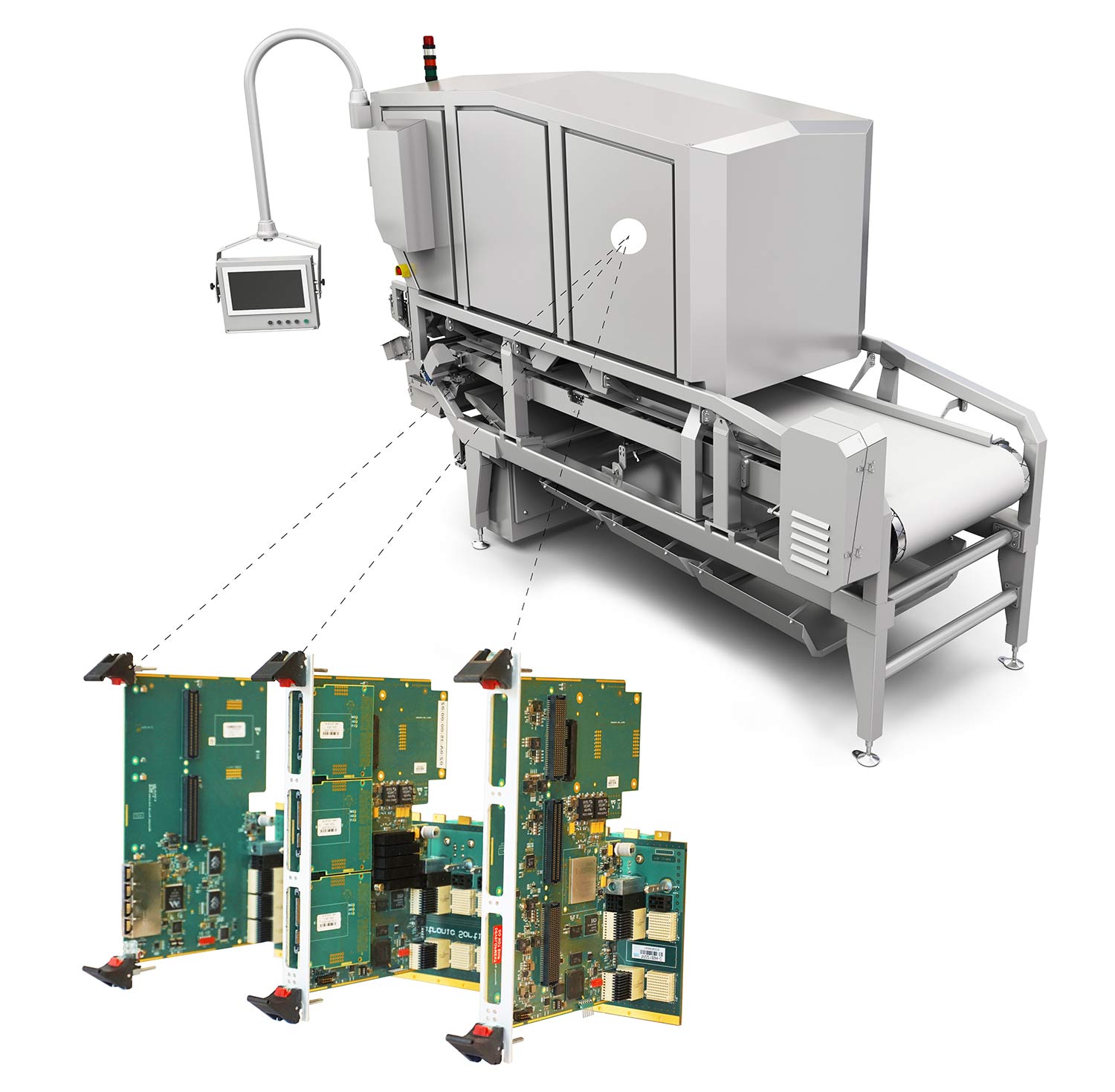
Closely related to the mechanical design, is our knowledge of the thermal management aspects of an embedded system. Thermal requirements can constrain the use of specific components or necessitate implementing a (custom designed) cooling solution.
A comprehensive system validation phase is also an important part of the system design process, in which the system is verified to comply with its original specifications. In addition, CE/FCC compliance tests, safety guideline checks, temperature and other environmental tests, like vibration and shock complete the validation process.
| Embedded system architecture |
| HW/FW/SW partitioning |
| Hardware development |
| Firmware development |
| Embedded software development |
| Operating system implementation |
| Driver development (e.g. PCIe, USB) |
| Application software development |
| Webserver functionality |
| Efficient processor – FPGA/SoC co-design |
| Mechanical design |
| Thermal design |
| CE/FCC & safety conformance |
| Environmental tests |
This validation step ensures that in the end, all subsystems of the embedded system work together seamlessly and efficiently performing according to specifications.
Hardware/Board Design
This approach assures that the board can be manufactured and tested efficiently, taking into account the technology and expected production volumes.
Signal integrity and power-integrity simulations

The signal-integrity (SI) and power-integrity (PI) simulations, provide confidence that the board fulfills the high speed signal requirements and power supply recommendations.
Test and validation